 |
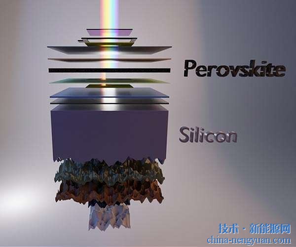
A research group of the American Nano Engineering Research Center (CRNE) and the researchers of the Department of Electronic Engineering of the University of Barcelona have jointly developed a more convenient and cheaper method for the preparation of crystalline silicon. Their research results were published in the latest issue of Applied Physics. This very thin silicon wafer has a thickness of about 10 microns, which is expensive but what microelectronics are expecting, especially with the development of three-dimensional integrated circuits for microchips. This is an inevitable choice. The development of silicon technology provides a broader perspective for the development of photovoltaic technology, especially for the development of flexible batteries.
In recent years, the development of technology has brought about a trend toward thinner silicon wafers. The thinnest silicon wafer thickness that wire cutting can bring is about 150 microns. The use of wire-cutting technology to obtain thinner silicon wafers is more difficult, but about half of the silicon material is lost during the cutting process. The research team's approach differs from general line cutting in that it can be achieved in one step and can produce wafers that are more efficient, faster, and less expensive.
This method is based on the production of many tiny pores on the surface of the material, and the process assists with high temperatures. The silicon segmentation process can precisely control the shape of tiny pores. The precisely controlled pore diameter not only controls the number of wafers but also precisely controls the thickness and deviation. This sandwich-like silicon wafer can be peeled off through the blade. The expected number and thickness of wafers can be controlled very accurately. CRNE scientists can easily divide a 300mm wafer into 10 thinner wafers, each between 5 and 7mm.
Reduce the cost of industrial production
The demand for ultra-thin wafers is increasing, and both the MEMES industry and the solar industry are in great demand. Traditional silicon cutting has reached a relatively bottleneck stage. The thickness of silicon wafers has grown from 300 mm in the 1990s to around 180 mm today, and the efficiency has been increasing and reducing costs. However, it is increasingly difficult to obtain thinner silicon wafers to further reduce costs. The emergence of this approach has solved this demand very well. Despite the thickness of tens of microns, the ability to absorb sunlight and perform photoelectric conversion remains.
bbq grill, bbq grill mesh, Grill Grate, stainless wire bbq grill,Bbq Grill Metal Mesh,etc. It is suitable for indoor and outdoor barbecue.
Barbecue wire grill grate is made of high quality 304 stainless steel, never rusting and durable. BBQ Wire mesh does not have any coating or chemical ingredients, making food safer.
Barbecue wire grill grate is made of high quality 304 stainless steel, never rusting and durable. BBQ Wire mesh does not have any coating or chemical ingredients, making food safer.
bbq grill mesh,stainless wire bbq grill,Bbq Grill Metal Mesh,cooking grate,bbq grill grates stainless steel
Shenzhen Lanejoy Technology Co.,LTD , https://www.szlanejoy.com