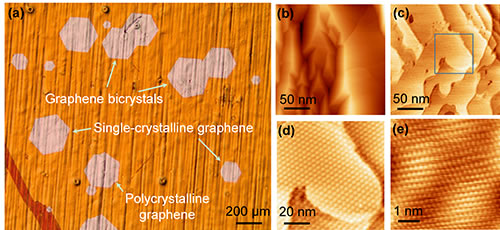
Figure 1. (a) Optical micrograph of graphene grown on copper foil by CVD method. (b)-(c) STM topography of graphene on copper foil. (d) The enlarged STM topographic map corresponding to the blue box area in (c) can see continuous Moore pattern. (e) Atomic resolution STM images at the Moore pattern in (d).
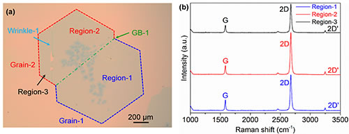
Figure 2. (a) Optical micrographs of bimorph graphene transferred to SiO2/Si substrates. (b) Raman spectra corresponding to the three regions in Figure (a).
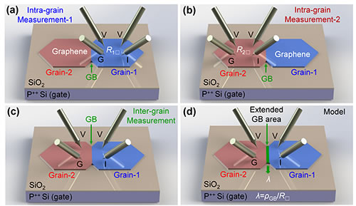
Figure 3. (a)-(b) Schematic representation of the four-probe method for measuring the crystalline domain transport properties on both sides of doubly graphene. (c) Four-probe transport test schematic across graphene grain boundaries. (d) A model diagram of the graphene grain boundary electrical resistivity and carrier mobility is obtained.
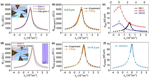
Figure 4. (a) Two-dimensional resistance vs. carrier concentration curves of the interior and intergranular boundaries (GB-1) of both crystalline domains on both sides of double crystal graphene. The insets are optical micrographs of cross-graphene grain boundary tests using the four-probe method. (b) Comparison curves of experimental data across grain boundaries and data fitted according to the model. (c) The resistivity of the three different graphene grain boundaries as a function of carrier concentration. (d) Transport test results across graphene wrinkles (Wrinkle-1) and a measured graphene domain. The illustration on the left is an optical micrograph of a graphene fold transport test. The illustration on the right shows an enlarged photomicrograph of this graphene fold. (e) Cross-folding transport test data versus a comparison curve based on data fitted to the model. (f) Graphene wrinkle resistivity as a function of carrier concentration.
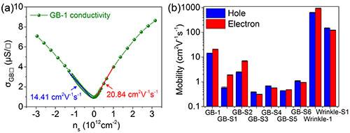
Figure 5. (a) Two-dimensional conductance at different carrier concentrations at the graphene grain boundary GB-S1. The hole and electron carrier mobility can be obtained by fitting a linear region on both sides of the curve. (b) Carrier mobility at the seven graphene grain boundaries and two graphene folds.
The quasi-particles (eg, exciton, Dirac fermion, etc.) of two-dimensional atomic crystal materials represented by graphene exhibit novel quantum properties such as room-temperature quantum Hall effect due to the quantum confinement effect, and also promote related new types of electrons. The application of optoelectronic devices and other related research. The key to obtaining intrinsic physical properties such as electrical transport properties, optoelectronic properties, and ultimately device applications is the growth of large-area, high-quality samples. In recent years, the research group of the Institute of Physics, Chinese Academy of Sciences/Beijing National Laboratory for Condensed Matter Physics (CIC) has obtained a series of research results in the controllable preparation of two-dimensional atomic crystal materials, the control of physical properties, and the study of prototype device characteristics. As early as in 2007, they obtained the first large-scale, almost defect-free, large-area, high-quality single-layer graphene on the surface of a metal germanium single crystal through an epitaxial method. In 2012, the semiconductor silicon material was successfully inserted between the graphene and the metal substrate to form a graphene/silicon/metal structure, thereby realizing the integration of graphene in the application of the electronic integrated device and the silicon-based technology. In 2015, they proposed and confirmed the intercalation mechanism of “silicon atom-induced defect-atom pass-defect self-repairâ€, revealing synergies between silicon atoms, graphene, and the substrate [J. Am. Chem] Soc. 137,7099 (2015). At the same time, they also achieved low barrier boron substitution and doping of epitaxial graphene on Ru (0001) at room temperature, which provided a valuable reference for the hole doping of graphene [Nano Lett. 15, 6464 (2015) )]. This series of results is of great significance for graphene electronics.
Another method for synthesizing graphene commonly used internationally is the use of chemical vapor deposition (CVD) to synthesize graphene on the order of millimeters or even centimeters in copper foil. However, graphene synthesized by the CVD method usually has Polycrystalline properties. The grain boundary between these polycrystalline graphene monodomains is composed of twisted six-membered rings and non-six-membered rings (five-membered rings, seven-membered rings, and eight-membered rings) on the microstructure. Carriers of graphene are When these defects are introduced, extra scattering is introduced, resulting in a decrease in the conductivity and mobility, which restricts the application of graphene in the field of electronic circuits. In general, people usually use two methods to characterize the transport properties of the graphene grain boundary. One is to make Hall electrodes using micromachining methods, and the other is based on scanning probe microscopy. The former will introduce pollution on the graphene surface, which will affect the intrinsic properties of graphene. The latter requires a lot of time to locate the graphene grain boundaries, such as the STP and KPFM. Therefore, how to quickly and non-destructively realize the measurement of the intrinsic electrical transport properties of graphene domains and grain boundaries is extremely challenging.
In order to effectively study the characteristics of intrinsic electrical transport in low-dimensional structures, the research team completely and thoroughly modified a commercial four-probe scanning tunneling microscope (STM) system, significantly improving the system's signal-to-noise ratio, mechanical and Temperature stability, imaging resolution, and cooling performance [Rev. Sci. Instrum., 88 (6) 063704, 2017]. Using a completely modified four-probe system, they performed transport tests on single crystal graphene transferred to SiO2/Si substrates. The van der Pauw method was reported for the first time to obtain graphene single crystal carrier mobility [ Chin. Phys. B, 26 (6) 066801, 2017]. Recently, the research group Dr. Ma Ruisong and associate researcher Bao Lihong used the four-probe STM to conduct systematic and in-depth research on the transport properties of graphene grain boundary electrical resistivity and mobility.
It was found that the size of graphene grown on copper foil by CVD method can reach the order of millimeters, including monocrystalline graphene, double crystallized graphene, and polycrystalline graphene with hexagonal shape. The characterization of a large number of STMs confirmed the continuity and high quality of graphene single crystal domains. The research work mainly focused on the double-crystal graphene transferred onto SiO2/Si substrate, so as to ensure the uniqueness of the grain boundary of the studied graphene. Raman measurements show the monolayer characteristics and low defect properties of the bimorph graphene. The researchers used the four-probe method to obtain graphene grain boundary electrical resistivity. First, they used the capacitance between the gate and the probe as feedback signals for the needles. Four STM probes were used as point-contact electrodes to measure the two-dimensional resistance of the crystalline domains on both sides of the double-crystal graphene and across the grain boundary. In order to extract the electrical resistivity of the graphene grain boundary, they established a grain boundary expansion model, ie, the graphene grain boundary is equivalent to a single crystal domain region with a certain width λ, and the internal and intergranular boundaries of both sides of the double crystal graphene are obtained. (GB-1) 2D resistance vs. carrier concentration curve. According to the extended model, they can well match the resistivity of the graphene grain boundaries at different carrier concentrations. In addition, they also applied this method to the transport test of graphene folds to obtain the resistivity of the folds. According to the resistivity at different carrier concentrations, the Drude transport model can be used to extract the carrier mobility at the grain boundary or wrinkle of graphene. The results show that the mobility at the grain boundary of the graphene is three to four orders of magnitude lower than that of the intrinsic graphene, and the mobility at the fold is about 1/6 to 1/5 of that at the intrinsic graphene.
This work extends people's understanding of intrinsic electron transport properties at the graphene grain boundaries/folds and demonstrates the unique advantages of the four-probe scanning tunneling microscopy system in studying the effects of microstructures, such as defects, on the transport properties of the material. It also provides a feasible method for characterizing the transport properties of grain boundaries in other two-dimensional materials.
The above results were recently published online in Nano Letters (DOI: 10.1021/acs.nanolett.7b01624). In this study, the Physics Institute team collaborated with the Liu Yunzhao Research Group of the Institute of Chemistry of the Chinese Academy of Sciences and Sokrates T. Pantelides, a professor at Vanderbilt University in the United States. The work was funded by the Ministry of Science and Technology, the National Natural Science Foundation of China, and the Chinese Academy of Sciences.
Solar Panels,Solar Panel Mono,Solar Power Panels
China Searun Solar Solution Co., Ltd. , https://www.searunsolar.com